Premium Only Content
The Steel Making Process From Start to Finish - Material Science
RCast iron pan manufacturing process
RMaking a Caterpillar Engine Block at the Mapleton, IL Foundry
RIntroduction to the Scanning Electron Microscope (SEM)
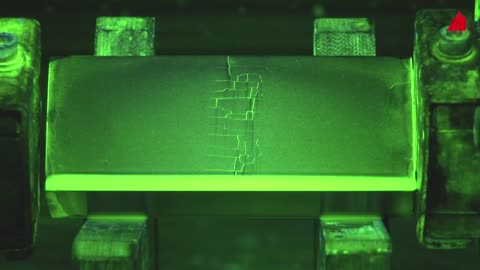
Magnetic Particle Inspection: Material Science
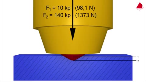
Vickers Hardness Test - Material Science
Metallography - Macroscopic Techniques - Material Science
Dye Penetrant Inspection - Material Science
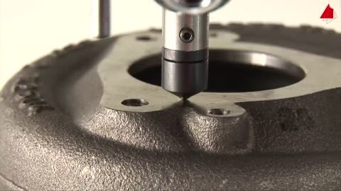
Brinell Hardness Test - Material Science
Rockwell Hardness Test: Material Science
Fatigue Test - Material Science
Material Science: Eddy Current Testing
Tensile Test: Material Science
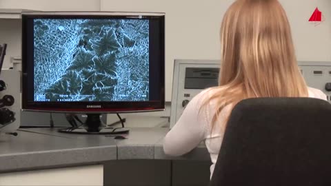
The Scanning Electron Microscope: Material Science
Microscopic Techniques - Metallography - Material Science
Material Science: X-ray Inspection and Industrial Computed Tomography
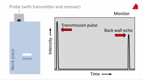
Ultrasonic Testing Basics: Material Science NDT
Introduction to the Scanning Electron Microscope (SEM)
Introduction to the Scanning Electron Microscope (SEM)
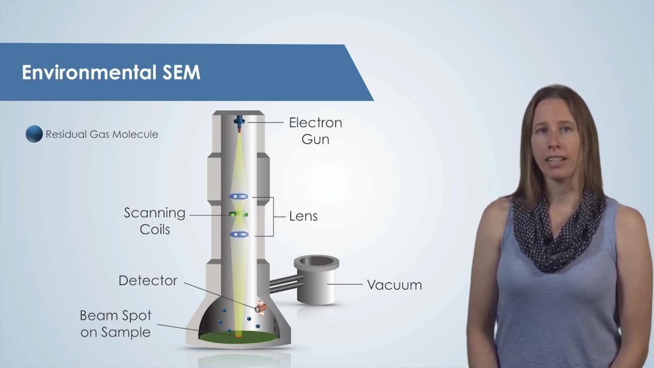
A scanning electron microscope (SEM) is a type of electron microscope that produces images of a sample by scanning the surface with a focused beam of electrons. The electrons interact with atoms in the sample, producing various signals that contain information about the surface topography and composition of the sample. The electron beam is scanned in a raster scan pattern, and the position of the beam is combined with the intensity of the detected signal to produce an image. In the most common SEM mode, secondary electrons emitted by atoms excited by the electron beam are detected using a secondary electron detector (Everhart–Thornley detector). The number of secondary electrons that can be detected, and thus the signal intensity, depends, among other things, on specimen topography. Some SEMs can achieve resolutions better than 1 nanometer.
More Material Science Videos
https://rumble.com/playlists/QExVxeOAGck
-
 DVR
DVR
TheAlecLaceShow
4 hours agoDoes Racism Exist? Guest: Franck Zanu | Elon’s Viral Meme | Hunter Pardon | The Alec Lace Show
5.07K3 -
 LIVE
LIVE
G2G Gaming Channel
6 hours agoI heard Smite, So Im here! #RumbleTakeOver #RumbleGaming
120 watching -
 15:36
15:36
Neil McCoy-Ward
2 hours ago🚨 Emergency Martial Law Declared, Special Forces Deployed...
12.7K5 -
 1:57:30
The Charlie Kirk Show
2 hours agoDemocrat Billionaires in Crisis + Fixing the Migrant Crisis | Blagojevich, O'Brien, Metaxas| 12.3.24
51.5K11 -
 1:01:07
The Dan Bongino Show
5 hours agoBiden’s Reign Of Destruction Isn’t Over Yet (Ep. 2381) - 12/03/2024
611K1.51K -
 1:59:02
Steven Crowder
5 hours ago🔴 COVID Chronicles: The Hidden Truths of the Pandemic Exposed
336K200 -
 LIVE
LIVE
SoundBoardLord
4 hours agoMulti-Gen Don Juan in Full Force!
168 watching -
 1:08:54
MTNTOUGH Fitness Lab
4 hours agoSheriff Mark Lamb Exposes America’s Border Crisis and Cartel Infiltration | MTNT POD#93
8.75K1 -
 8:52
8:52
Cooking with Gruel
12 hours agoToasted Brown Butter Cornbread
10.8K -
 1:01:44
The Rubin Report
3 hours agoJon Stewart Loses His Cool with Democrats for Saying This About Hunter Biden Pardon
49.7K60


