Premium Only Content
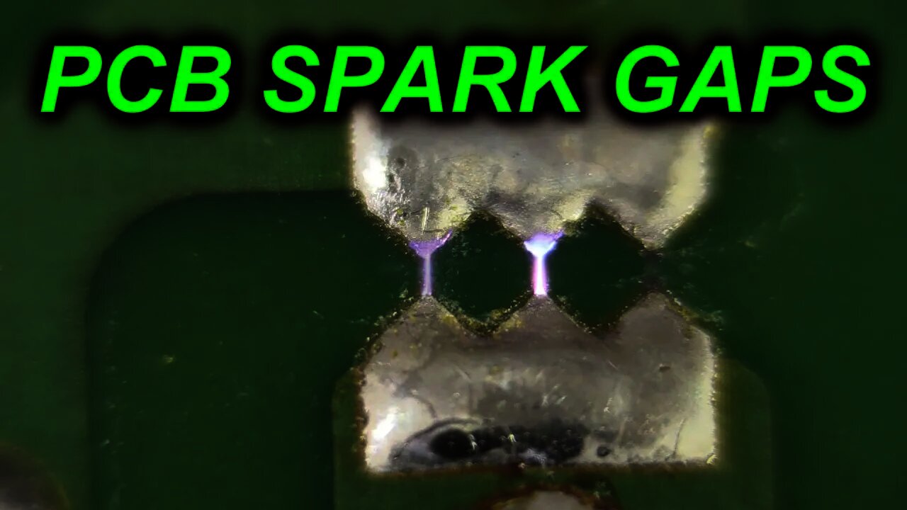
EEVblog #678 - What is a PCB Spark Gap?
In this tutorial Dave explains what a PCB spark gap is and how it can be a useful zero cost addition to your PCB layout to help prevent ESD damage.
He shows how to easily design them into your board and calculate the approximate voltage rating.
And of course has some fun applying 5kV to some gaps to show how them at work.
Plugpack teardown: https://www.youtube.com/watch?v=_EMAggN5H-w
Support the EEVblog through Patreon!
http://www.patreon.com/eevblog
Forum: http://www.eevblog.com/forum/blog/eevblog-678-what-is-a-pcb-spark-gap/
EEVblog Main Web Site: http://www.eevblog.com
The 2nd EEVblog Channel: http://www.youtube.com/EEVblog2
EEVblog Amazon Store (Dave gets a cut):
http://astore.amazon.com/eevblogstore-20
Donations:
http://www.eevblog.com/donations/
Projects:
http://www.eevblog.com/projects/
Electronics Info Wiki:
http://www.eevblog.com/wiki/
-
 5:24
5:24
EEVblog Channel
4 months ago $0.04 earnedEEVblog Random LIVE
245 -
 19:50
19:50
EEVblog Channel
6 years agoEEVblog #1082 - What Do Compliance Logos Mean?
37 -
 25:33
25:33
EEVblog Channel
4 years ago $0.01 earnedEEVblog #1283- What is Mains Ripple Injection?
34 -
 5:31
5:31
EEVblog Channel
6 years agoEEVblog #1070 - What The Hack? Dumpster Hacking!
6 -
 19:53
19:53
EEVblog Channel
4 years agoEEVblog #1295 - What Makes A Good Lab HEPA Air Filter?
9 -
 9:23
9:23
EEVblog Channel
7 years agoEEVblog #996 - What Is The CE Mark On A Product?
14 -
 18:29
18:29
EEVblog Channel
9 years agoEEVblog #732 - PCB Sheet Resistance
8 -
 34:27
34:27
EEVblog Channel
7 years agoEEVblog #1029 - BGA PCB Fanout
14 -
 19:09
19:09
EEVblog Channel
7 years agoEEVblog #1036 - PSU Fire PCB Repair
21 -
 1:09:58
EEVblog Channel
5 years agoEEVblog #1259 - PCB Manufacturing Options EXPLAINED
30